ElectronParade
Welcome to Lesson 175! In our last lesson, we explored Electronic Design Automation (EDA) software like EasyEDA and KiCad, and we built our very first digital schematic. A schematic is a logical map of your circuit, but it is not a physical object.
Today, we cross that bridge. We are going to take the schematic we designed and convert it into a Printed Circuit Board (PCB) layout. This is the exact process professional hardware engineers use to design the motherboards, graphics cards, and flight controllers that run the modern world.
The Workflow: From Logic to Physical Space
In EDA software, the transition from schematic to PCB layout is usually a single button click (often labeled “Update PCB from Schematic”). When you do this, your software takes all the abstract symbols (resistors, ICs, LEDs) and replaces them with their physical footprints.
A footprint is the exact 2D shape of the component as it will sit on the board, including the exact size and spacing of the copper pads required to solder it down.
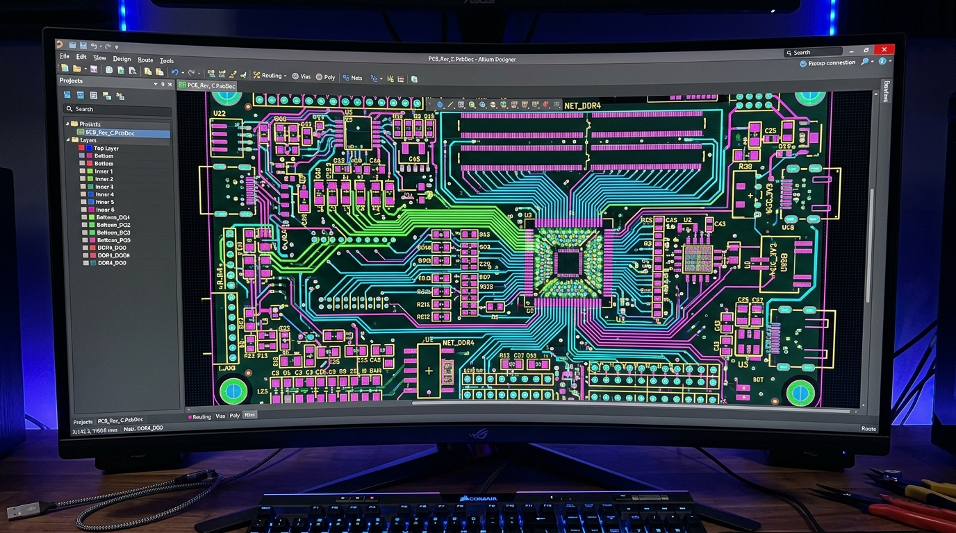
When you first open your PCB layout, you will see a mess of components piled on top of each other, connected by thin, criss-crossing lines called the ratsnest.
Step 1: Component Placement
Routing a board is 90% placement and 10% routing. If you place your components well, drawing the traces will be effortless. If you place them poorly, you will end up with a tangled nightmare.
Here are the golden rules of component placement:
- Fixed Components First: Place things that must interact with the outside world first. USB ports, power jacks, switches, and mounting holes should be locked into position immediately.
- Follow the Flow: Try to place components in a way that mimics the logical flow of your schematic. If a signal goes from a sensor to a microcontroller to an LED, place them in roughly that order physically.
- Keep Decoupling Capacitors Close: If you have a 100nF decoupling capacitor for an IC, place it as close to the IC’s power pin as physically possible. Its job is to filter high-frequency noise right at the source.
- Group Sub-Circuits: If you have a power regulation section (a voltage regulator, a diode, and some bulk capacitors), group them tightly together in one corner of the board.
Step 2: Routing the Traces
Once your components are placed, the ratsnest lines will show you what needs to be connected. Your job is to replace those abstract lines with actual copper traces.
Think of traces as flat wires painted onto the fiberglass board.
Trace Widths
Not all traces are created equal. A trace carrying 5 Volts at 2 Amps to a motor needs to be much wider than a trace carrying a low-current data signal.
- Data signals: 0.2mm to 0.3mm (8 to 12 mils) is standard.
- Power traces: 0.5mm (20 mils) or wider, depending on the current. There are many free trace width calculators online that will tell you exactly how wide a trace needs to be to safely carry a specific current without melting.
Routing Etiquette
- Use 45-Degree Angles: Never route traces at sharp 90-degree angles. They can cause acid traps during the manufacturing process and signal reflections at high speeds. Always use 45-degree bends.
- Top and Bottom Layers: A standard, cheap PCB is “2-layer”, meaning it has copper on the top and the bottom. Use the top layer for vertical routing and the bottom layer for horizontal routing (or vice versa).
- Vias: When a trace on the top layer gets blocked by other traces, you can place a Via—a tiny plated hole that connects the top copper to the bottom copper—allowing your signal to tunnel under the obstacle.
Step 3: Copper Pours (Ground Planes)
Instead of routing dozens of individual traces for your Ground (GND) connections, it is standard practice to create a Copper Pour.
You draw a massive rectangle around the entire board and assign it to the GND net. The software will fill the empty space on the board with solid copper and automatically connect all GND pins to it. This provides a low-impedance return path for your entire circuit and acts as a giant heat sink. Usually, designers pour ground on both the top and bottom layers.
Step 4: The Design Rule Check (DRC)
Before you declare victory, you must run the DRC (Design Rule Check).
The DRC is a built-in tool that scans your entire board looking for physical impossibilities or manufacturing violations. It checks for:
- Clearance: Are two traces too close together? (If they touch during manufacturing, it will create a short circuit).
- Unrouted Nets: Did you forget to route a connection? The DRC will flag any remaining ratsnest lines.
- Silkscreen over Pads: Did you accidentally place text over a soldering pad?
Never manufacture a board until your DRC reports zero errors.
Up Next
You now have a fully routed, error-free PCB design sitting on your hard drive. But it’s still just digital files. In our next lesson, we will learn how to generate Gerber files—the universal language of PCB manufacturing—and send them to a fabrication house in China to turn our digital dreams into physical silicon and fiberglass.